On-Die Power Rail Measurements: Setup and Best Practices
Accurate on-die power rail measurements depend on proper sense-line design, differential probing, and careful test setup at the package level.
Accurate on-die power rail measurements depend on proper sense-line design, differential probing, and careful test setup at the package level.

Transmission line losses—driven by skin effect and dielectric properties—play a critical role in degrading high-speed signal integrity and eye performance.
Transmission line loss directly affects eye diagram quality, with around −12 dB at Nyquist marking the limit before signal integrity rapidly degrades without equalization.
Understanding PCIe’s layered architecture reveals why capturing synchronized physical- and protocol-layer behavior is essential for effective link debugging.


Peripheral Component Interconnect Express (PCIe®) is a high performance, general-purpose input/output (I/O) interconnect designed for a wide variety of computing and communication platforms. Recent iterations of the standard take advantage of high-speed serial technology, point-to-point interconnects, switch-based technology, and packetized protocol. They rely heavily on link negotiation and link training, so much so that being able to capture and view dynamic link behaviors is essential to debugging PCIe devices. Nevertheless, it remains a pain point for PCIe engineers. Why is it so difficult? To start, let’s break down the PCIe architecture to understand what is going on.
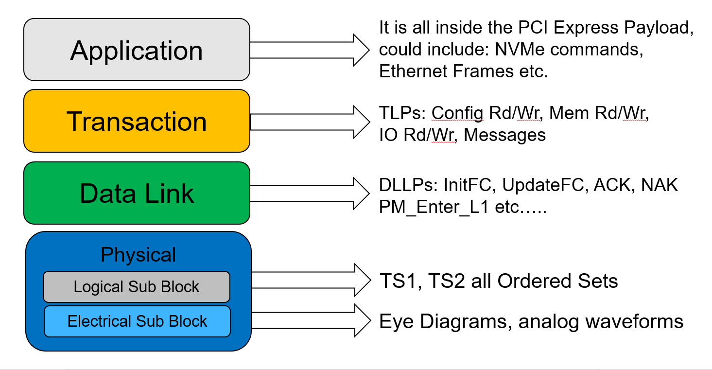
The PCIe architecture uses a layered design (Figure 2), similar to the seven-layer OSI structure in network communication.
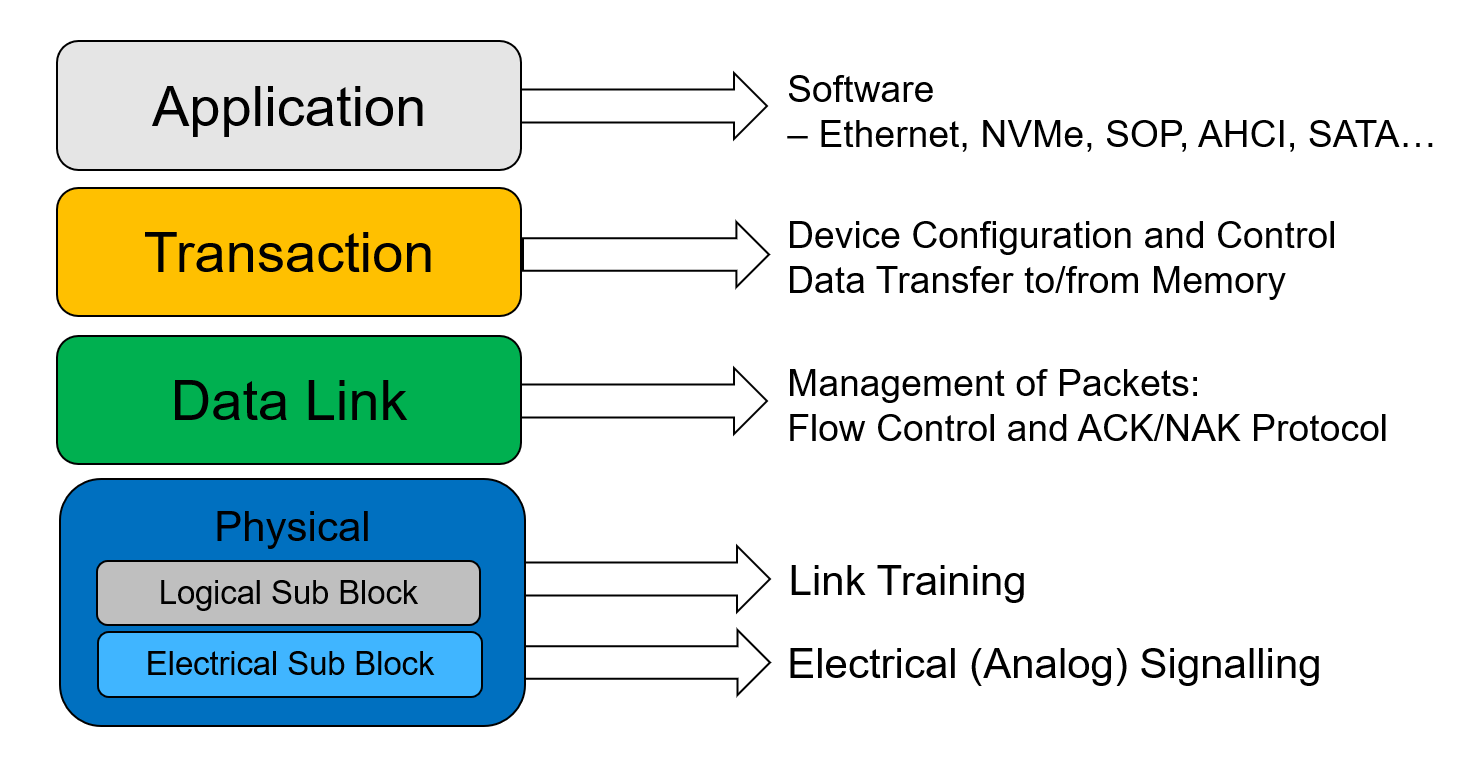
The application layer (or host layer) is really beyond the scope of what the PCIe specification would cover. That is where protocols like Ethernet, Non-Volatile Memory Express (NVMe) and others appear in the form of payload. The PCIe protocol doesn’t much care what is in the payload, rather it defines a method of transferring that data across a link.
The transaction layer is used for configuring devices on the link. Think of it as a method of transferring memory from host memory to the device and vice versa. It has commands for configuring memory reads and writes, which is basically configuring and numerating the device then transferring data back and forth. It also has mechanisms for message and error reporting.
The transfer of data between those devices is managed by the data link layer. That is where the flow control mechanism and the acknowledgement protocol reside to ensure the integrity of packets going across the link. The data link layer also manages entry into low power states, telling the physical layer, "I want to go to sleep now and save power."
At the lowest level, the physical layer is broken into two sub-blocks, the electrical sub-block and the logical sub-block. The electrical sub-block implements the analog components required for all analog signaling. The logical sub-block controls how the two devices actually talk to each other, using state machines for establishing a link. It generates ordered data patterns, including training sequences which are exchanged with other devices during link training.
Figure 3 shows the messages and commands you would typically see at each layer.
When two PCIe devices talk to each other, they are considered a link. Each side has a transmitter (TX) and a receiver (RX) as shown in Figure 1 above.
When you connect a root complex/host to an endpoint, the application layer software tries to transfer data between itself and the endpoint using this PCIe link as a transport. The device driver that is aware of the application software from above will create the PCIe traffic and pass it through the transaction layer to the datalink layer to the physical layer and across to the other side of the link.
Problems arise because layers do not have “visibility” into the actions of layers more than one level above or below them. For example, the flow control and error correction actions of the data link layer would be transparent to the application layer, but they could potentially affect performance.
Another problem is that different test equipment is used to access transactions at different layers. Oscilloscopes are used to acquire and display the physical layer electrical signals and lower-level logical operations. Protocol analyzers record and display all the higher-level logical operations. The acquisitions these instruments make are on vastly different time scales, from perhaps milliseconds for an oscilloscope to minutes for a protocol analyzer. Also, they have very different displays, oscilloscopes producing waveform traces, eye diagrams and other analog signal information, with perhaps some decoding of logical sub-block data. Protocol analyzers show information about serial data packets, with perhaps some symbol/bit-level decoding of the packets. Even if you could make perfectly time-correlated oscilloscope and protocol analyzer acquisitions, it would not be immediately apparent how those acquisitions corresponded to one another.
The only way to achieve total PCIe link visibility is to link the operation of an oscilloscope and protocol analyzer—which is exactly what CrossSync™ PHY for PCIe does. We’ll talk more about how in the next post.
Copyright © 2020-2026 Teledyne LeCroy. All rights reserved. All original content, including text and photos, is the property of Teledyne LeCroy and cannot be reproduced without expressed written permission.

CrossSync PHY enables time-synchronized protocol and oscilloscope analysis to diagnose unexpected PCIe link equalization and preset training behavior.


CrossSync PHY enables time-synchronized oscilloscope and protocol analysis to verify PCIe L1 substate clock request and reference clock timing.

PCIe 6.0’s move to PAM4 signaling introduces new compliance pattern measurements—SNDR, RLM, and ps21TX—that require updated test methodologies and noise-aware analysis.

PCIe 6.0 compliance requires SNDR and RLM results with oscilloscope noise removed—these three methods show how to compensate noise accurately in real test setups.