On-Die Power Rail Measurements: Setup and Best Practices
Accurate on-die power rail measurements depend on proper sense-line design, differential probing, and careful test setup at the package level.
Accurate on-die power rail measurements depend on proper sense-line design, differential probing, and careful test setup at the package level.

Transmission line losses—driven by skin effect and dielectric properties—play a critical role in degrading high-speed signal integrity and eye performance.
Transmission line loss directly affects eye diagram quality, with around −12 dB at Nyquist marking the limit before signal integrity rapidly degrades without equalization.
Sharp dips in S-parameter plots often indicate coupling to high-Q resonant structures, where specific frequencies are absorbed by PCB cavities or floating interconnects.

The last pattern we'll cover in this series on reading S-parameters is sharp dips. These dips result from coupling to high-Q resonant structures and represent very narrowband absorption in S21 or S11.
Where do you see resonant coupling? Resonant structures can include coupling to an interconnect that is floating and not terminated. The structure does not have to be a uniform transmission line, it can also be a cavity made up of two or more adjacent plates as shown in Figure 1. Commonly, when a signal goes through a cavity and we hit the resonances of the cavity, it absorbs energy and results in narrow dips in the S-parameters.
In Figure 1, the signal goes through a via from top to bottom. The return current has to make the transition from the upper to the lower return plane. If the return path is not well controlled and is not in close proximity to the signal lines, the return current gets coupled into that cavity and we see that the energy of those resonant frequencies sucked out of the signal that gets transmitted.
Let’s look at a real-world example shown in Figure 2.
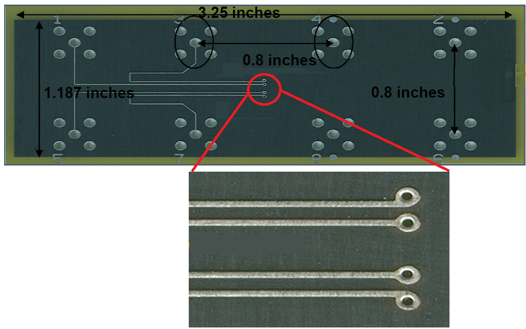
This FR4 printed circuit has eight symmetrically spaced ports using SMA connectors. We’ll focus on the micro-strip transmission line connecting port 1 on the top layer to port 2 on the bottom layer. The signal line makes the transition through the vias in the center of the board, shown in the exploded view. Note that there are no associated return vias. The return current has to make the transition from the upper internal layer to the lower internal layer, and in doing so it excites the resonance of the cavity formed by those layers. The frequencies of the resonances, based on the board dimension and the dielectric constant of the board material, can be predicted by the equation:

The principal modes are defined by the length and the width of the board. Another resonant mode is defined by the spacings of the SMA connectors, where the connector grounds short the internal planes. Using the given equation, we can calculate the resonant and list the expected frequencies.
| Length (in) | Resonant Frequency (GHz) |
|---|---|
| 3.25 | 0.92 |
| 1.187 | 2.5 |
| 0.8 | 3.75 |
Now let’s look at the measurement of S21 for this board (in Figure 3).
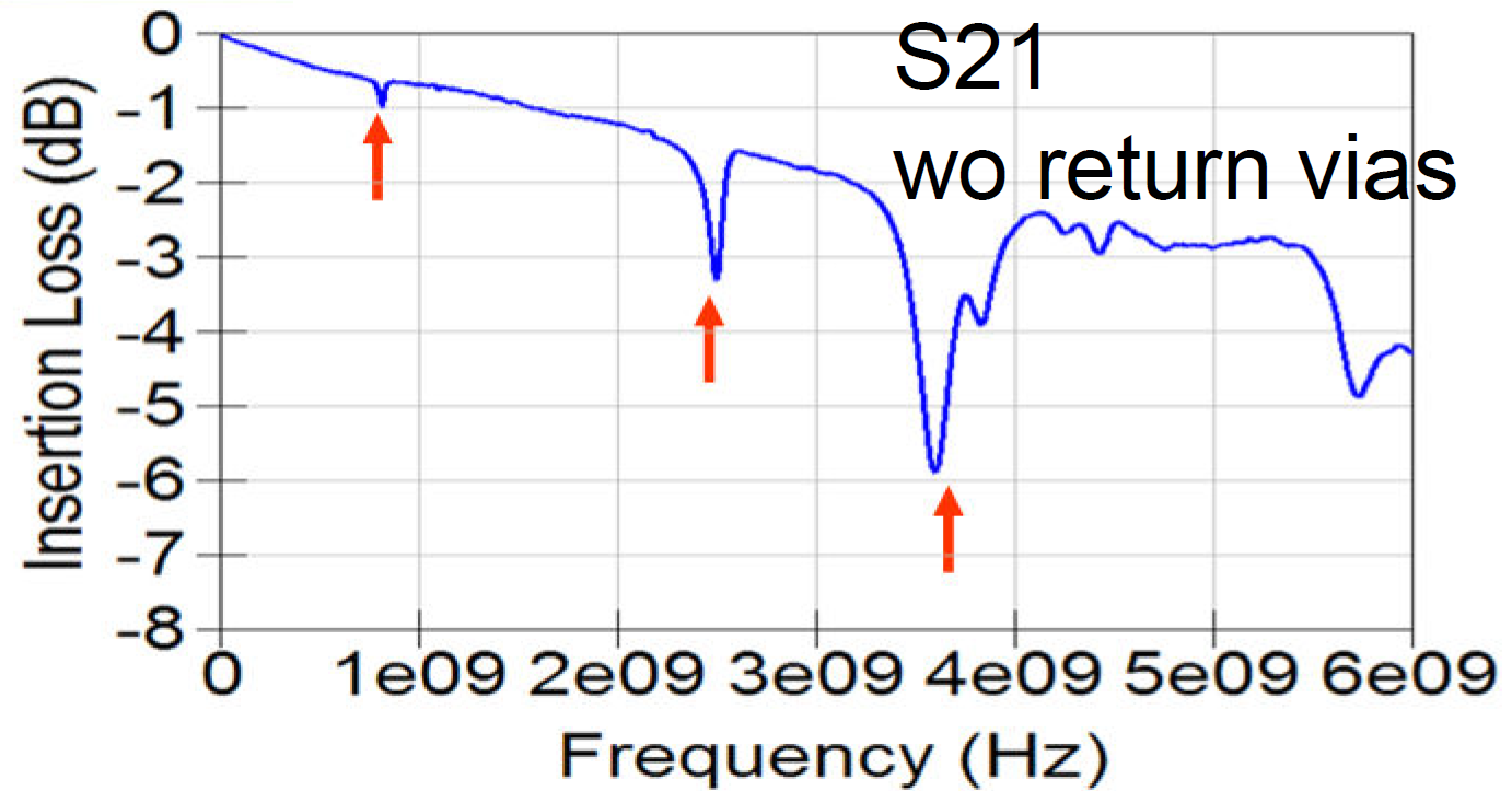
As expected, we see that S21 at low frequency is 0 dB. There is the monotonic slope due to resistance and dielectric losses. And we see the three sharp dips related to the coupled resonances we calculated at 0.92, 2.5 and 3.75 GHz.
The Q of the resonance is the ratio of the resonant frequency to the width at half the maximum. The resonance at 2.5 GHz has a width of about 0.1 GHz, so the Q is 25. Q’s of more than 10 are considered high.
The depth of the dips due to resonant coupling depends on the degree of coupling. The dip at 0.92 GHz has the smallest dip because the via in the port1 to port 2 path is symmetrically spaced at the center of the board length. Energy propagates equally to the left and to the right and the equal reflections cancel each other. If the via had been at either end of the board, the coupling would be greater. The via is closer to the upper edge of the board, and this asymmetry forces a higher degree of coupling for the resonant dip at 2.5 GHz. There are multiple resonances for the 0.8 inch spacing, and the via is not particularly symmetric with most of them, so the coupling is greater.
Eliminating these dips requires careful design. First, you should try to avoid transitioning the signal between different return planes. If you must, use return vias adjacent to each signal via to suppress resonance.
Copyright © 2020-2026 Teledyne LeCroy. All rights reserved. All original content, including text and photos, is the property of Teledyne LeCroy and cannot be reproduced without expressed written permission.

Mixed-mode S-parameters are derived from single-ended measurements through matrix transformations that reveal differential and common-mode signal behavior.

Mixed-mode S-parameters provide a powerful framework for analyzing how differential and common signals interact in complex transmission systems.

Mode conversion in differential signaling is driven by asymmetry between signal paths, revealing itself through mixed-mode S-parameters.

Understand how ripple patterns and resonance effects in S-parameters expose impedance mismatches, interconnect length, and signal integrity behavior.