On-Die Power Rail Measurements: Setup and Best Practices
Accurate on-die power rail measurements depend on proper sense-line design, differential probing, and careful test setup at the package level.
Accurate on-die power rail measurements depend on proper sense-line design, differential probing, and careful test setup at the package level.

Transmission line losses—driven by skin effect and dielectric properties—play a critical role in degrading high-speed signal integrity and eye performance.
Transmission line loss directly affects eye diagram quality, with around −12 dB at Nyquist marking the limit before signal integrity rapidly degrades without equalization.
Wide-bandgap power devices demand high bandwidth and superior CMRR, making probe selection critical for accurate high-voltage upper-side measurements.


In another post, we introduced you to a new tool on the Teledyne LeCroy website: The High-voltage Probe Selection Guide. To demonstrate the benefits of the guide, let’s explore further what must be considered when choosing an HV oscilloscope probe for power semiconductor device measurements.
Why are power semiconductor device measurements challenging?
Measuring both upper and lower power semiconductor devices simultaneously gives complete insight into the design’s behavior. In addition to evaluating the switching losses, designers will evaluate the timing to learn if there is sufficient dead-time margin to preclude any possibility of both upper and lower devices being turned on at the same time, which would cause a short circuit (shoot through). So, it's essential to have a probe that can perform adequately for the upper side measurements.
Choosing with the High-voltage Probe Selection Guide
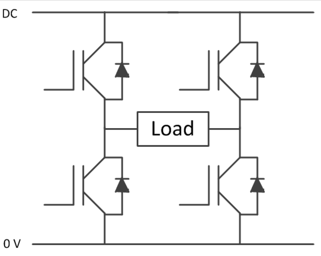
The circuit to be tested is a full-bridge topology using four wide- bandgap (GaN in this case) metal oxide semiconductor field effect transistors (MOSFETs). The desired measurement is to determine the switching losses of the MOSFETs. There are two lower side MOSFETs and two upper side MOSFETs, as shown in Figure 2.
Based on this information, we make three, simple selections on the High-voltage Probe Selection Guide (Figure 3):
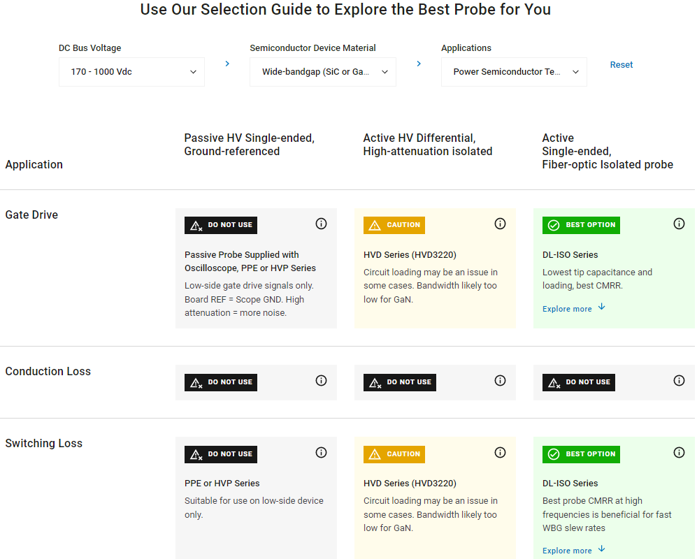
The Guide chooses the DL-ISO Series High-Voltage Optically Isolated Probe as the best probing option (green) for the gate drive and switching loss measurements.
The HVD Series High-Voltage Differential Probe is a better option than a single-ended passive probe, but it may cause circuit loading due to its input capacitance. It may also have insufficient bandwidth for the faster wide bandgap devices, especially the GaN device used in the example. There are compromises in using this type of probe, but some users may find that the probe works fine for their particular measurement needs.
One reason the DL-ISO is the best option is the probe’s CMRR. The DL-ISO series has a CMRR of 160 dB at DC and significantly higher CMRR than the other probes at higher frequencies. The HVD probe has a CMRR of 85 dB at DC and 65 dB at 1 MHz. While the HVD Series probe has excellent CMRR for a conventional HV differential probe, and may perform acceptably well depending on the device and the circuit, CMRR is not as good as DL-ISO, and it has much less than 1 GHz bandwidth.
Finally, the DL-ISO Series offers up to 1 GHz bandwidth to match the requirements of GaN devices. The HVD Series probes have a bandwidth of up to 400 MHz, corresponding more closely to the bandwidth requirements of SiC or Silicon (Si) power semiconductor devices.
The best choice for this type of power device measurement is the single-ended, fiber optically isolated probe. Its single-ended configuration minimizes loading, which offers the benefit of better signal fidelity. The probe isolation circuitry is less susceptible to picking up transients. It has better CMRR at high frequencies, which is important for circuits using wide bandgap semiconductors such as the GaN MOSFETs in this example. This, combined with the probe’s isolation circuitry, results in more accurate upper side measurements.
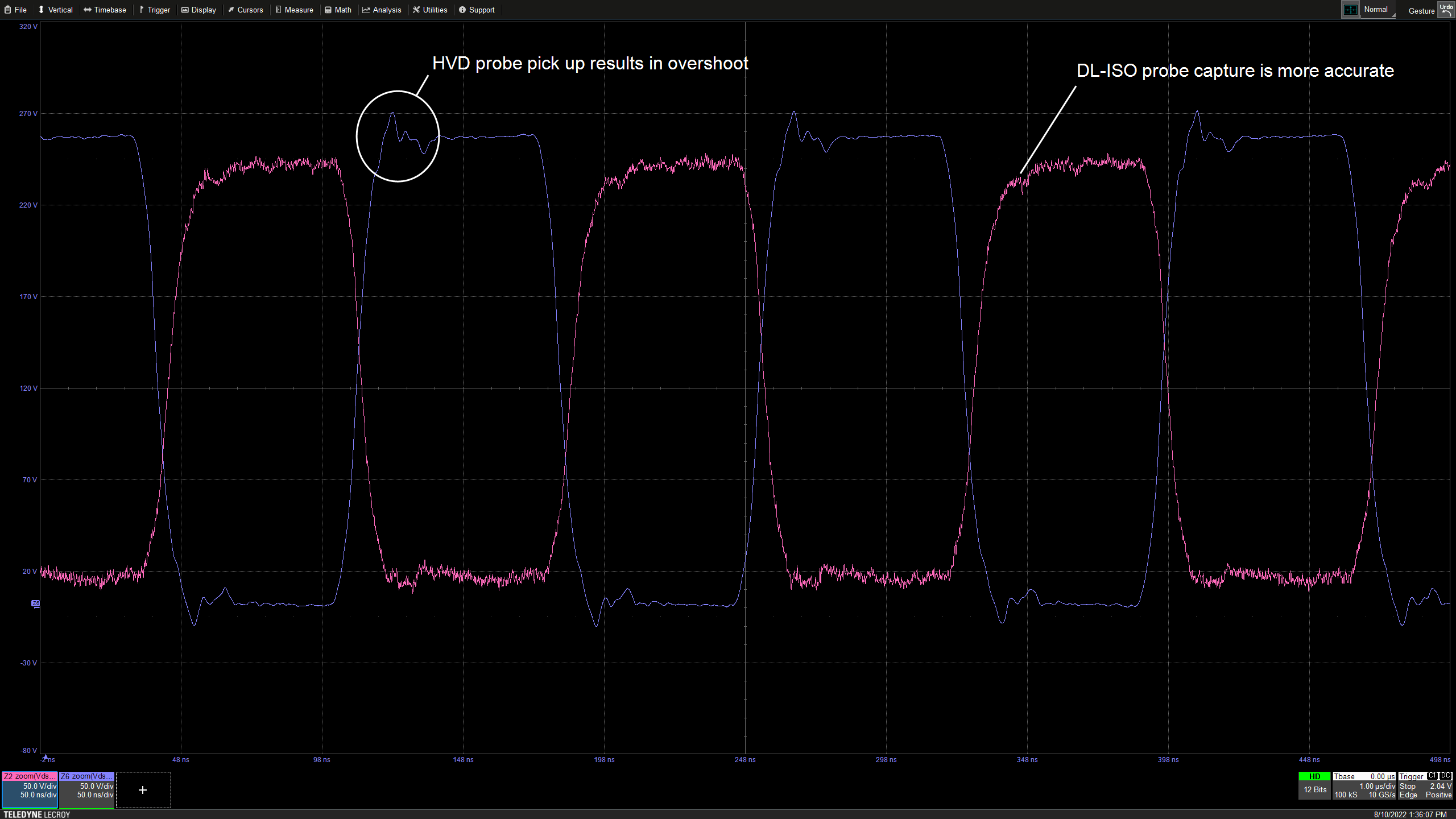
To prove the point, let’s compare Vds (MOSFET Drain-Source) signals captured using a DL-ISO probe and an HVD probe (Figure 1). The DL-ISO probe (magenta trace) is connected to the gate of one of the upper side MOSFETs. The HVD probe (blue trace) is connected to the gate of the other upper side MOSFET. This allows simultaneous observation without the probes affecting each other by loading the circuit, which would happen if they were connected to the same measurement point.
Note that the HVD probe exhibits a small overshoot on the edge transitions. This overshoot is most probably due to the lower CMRR of the HVD probe compared to the DL-ISO. There is no discernible overshoot visible in the signal from the DL-ISO probe. The optical coupling of the DL-ISO probe provides the best CMRR performance, which helps to suppress electrical transients coming from elsewhere in the circuit.
Copyright © 2020-2026 Teledyne LeCroy. All rights reserved. All original content, including text and photos, is the property of Teledyne LeCroy and cannot be reproduced without expressed written permission.
Learn more about the Teledyne LeCroy's optical and other High Voltage probes by visiting this Power Electronics Probes page.

Understanding the internal design of a 10x passive probe reveals the trade-offs that affect signal accuracy, bandwidth, and noise performance.


Knowing a probe’s dynamic range, differential limits, and common-mode voltage helps ensure safe and accurate measurements in high-voltage circuits.

Attaching multiple probes to the same test point can cause probe loading and interference, leading to inaccurate oscilloscope measurements and distorted waveforms.

CAT ratings define measurement safety based on source impedance and location—not probe performance or measurement accuracy.