On-Die Power Rail Measurements: Setup and Best Practices
Accurate on-die power rail measurements depend on proper sense-line design, differential probing, and careful test setup at the package level.
Accurate on-die power rail measurements depend on proper sense-line design, differential probing, and careful test setup at the package level.

Transmission line losses—driven by skin effect and dielectric properties—play a critical role in degrading high-speed signal integrity and eye performance.
Transmission line loss directly affects eye diagram quality, with around −12 dB at Nyquist marking the limit before signal integrity rapidly degrades without equalization.
This article explains how PDN design, probing method, and measurement location influence power rail noise—and why board-level measurements can be misleading.

Excerpted by permission from the Signal Integrity Journal article, Measuring Only Board-level Power Rail Noise May Be Misleading
In our blog, we’ve presented a lot about the impact of the interconnect on oscilloscope measurements, and how where you probe can be as important as how you probe. This article is an excellent demonstration of those very principles.
Power rail measurements are important because they can identify potential sources of noise before they become a problem. However, measuring only the power rail noise at the board-level may be a misleading indication of the noise the die actually sees.
Measuring a power rail on a board seems like a simple task. Like all measurements, it is easy to get a waveform on the oscilloscope’s screen, but it is difficult to have confidence you have eliminated the measurement artifacts and have a realistic measure of the actual signal present.
For example, the type of probe used to connect between the board/device under test (DUT) and the oscilloscope plays an important role. If you use a 10x probe, the tip loop inductance can act like an antenna and pick up RF noise either from the external environment, or from the near-field environment of the power rail itself. Figure 1 shows the voltage on a 3.3 V switch-mode power supply (SMPS) measured with a 10x probe, and the pick-up noise from an adjacent 10x probe shorted to itself, acting like an RF antenna.
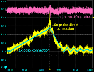
In this example, an independent measurement of the power rail voltage was made at the same location as the 10x probe using a coaxial connection on the board with a coax cable directly into the oscilloscope. This connection did not pick up any external or near-field radiated emissions, and it did not attenuate the signal by a factor of 10 like the 10x probe did. This is an example of the impact different probing methods can have.
Even with a good probing methodology, where you measure the power rail influences the noise you measure. It is important to always keep in mind that once the interconnects provide the correct connectivity, all they can do is add noise. Our job in designing the interconnects is to reduce the noise generated by the interconnects to an acceptable level.
In the power distribution path, the dominant parasitic introduced by the interconnects is inductance due to the loop inductance of the power and return conductors. The combination of the interconnect’s loop inductance and the discrete capacitors added to the power distribution network create embedded low-pass, LC filters.
Even though every conductor tied to the power rail is nominally the same net, the noise you would measure on different nodes of the power rail on the board will not be the same. What you measure depends on where the noise is measured. It depends on the victim; where the noise is generated, the aggressor; the frequency components of the noise; and the low-pass filters between the aggressor and the victim nodes.
Figure 2 is a simplified view of the PDN showing some of these low-pass filters.
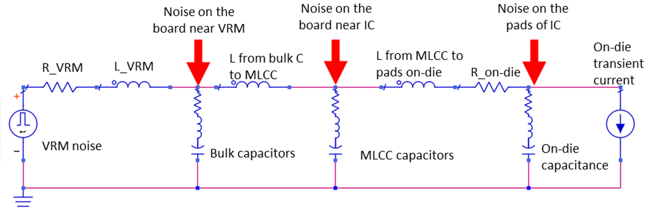
Depending on the nature of the interconnects and the discrete decoupling capacitors, the pole frequency of the LC filters might range from a low of 10 kHz to a high of 10 MHz. For example, if the source of the noise is 50 kHz frequency components from the switching noise of the VRM, the higher frequency components may not be seen on the die, but some of the 50 kHz components may get through.
If the aggressor is the transient current from the die, the voltage noise on the die when depleting the on-die capacitance will drive dI/dt currents through the package lead inductance. While this noise will be measured on the die, since it generally has high frequency components, it will be filtered by the time it gets through the low-pass filters of the package lead inductance and board-level decoupling capacitors. It may not appear on a node on the board-level power rail.
To demonstrate this principle, I designed a simple board that creates on-die power rail noise from switching currents while allowing a direct measure of the on-die power rail voltage and the board-level power rail voltage. The circuit is just a simple clock that drives four of the inputs to a hex inverter chip. The other two pins of the hex inverter are used to measure the on-die voltages.
The use of the board is demonstrated in another post, Signal and Power Integrity Tutorial: Power Rail Probing for Rail Compression
Copyright © 2020-2026 Teledyne LeCroy. All rights reserved. All original content, including text and photos, is the property of Teledyne LeCroy and cannot be reproduced without expressed written permission.
Copyright © 2020-2026 Teledyne LeCroy. All rights reserved. All original content, including text and photos, is the property of Teledyne LeCroy and cannot be reproduced without expressed written permission.

Accurate on-die power rail measurements depend on proper sense-line design, differential probing, and careful test setup at the package level.

Transmission line losses—driven by skin effect and dielectric properties—play a critical role in degrading high-speed signal integrity and eye performance.

Transmission line loss directly affects eye diagram quality, with around −12 dB at Nyquist marking the limit before signal integrity rapidly degrades without equalization.

This tutorial explains how quiet I/O probing reveals true on-die rail compression—often far greater than what traditional board-level measurements show.